Materials Engineer Jobs

1,587 jobs found — updated daily

Senior/Staff Advanced Packaging Materials Engineer, Texas Institute for Electronics

The University of Texas at Austin•Austin, TX
•Onsite

About The Position

The Texas Institute for Electronics (TIE), a University of Texas at Austin-supported semiconductor consortium, develops a state-of-the-art 3D heterogeneous integration manufacturing technology roadmap and provides pilot manufacturing capabilities. This position develops new formulations and evaluates existing materials for advanced packaging products. The engineer works with process development teams, internal partners, and external vendors to identify material candidates and solutions, and develops comprehensive testing and characterization plans for internally developed and externally acquired materials. The position may be filled at the Senior Engineer level or higher, depending on experience and qualifications. The work focuses on material development, characterization, qualification, and process optimization for advanced semiconductor packaging technologies, including 2.5D/3D integration, heterogeneous and mixed-material integration, and hybrid bonding. The engineer collaborates with engineering, manufacturing, equipment development, customers, suppliers, and industry partners to translate technical requirements into material specifications, development roadmaps, and practical solutions. The role is based on-site in a scientific research and prototyping facility in Austin, Texas, with occasional work outside standard office hours potentially required during peak periods and special events.

Requirements

  • For the Senior Engineer level: Bachelor’s degree in Polymer Science, Materials Science and Engineering, or a closely related engineering discipline, plus two years of experience in the semiconductor packaging industry or a closely related industry; alternatively, a master’s degree or higher in one of these fields.
  • For the Staff Engineer level: Bachelor’s degree in Polymer Science, Materials Science and Engineering, or a closely related engineering discipline, plus five years of experience in the semiconductor packaging industry or a closely related industry; alternatively, a master’s degree in one of these fields plus three years of relevant industry experience, or a Ph.D. or higher in one of these fields.
  • Experience in the semiconductor packaging industry or a closely related industry.
  • Hands-on experience in semiconductor packaging materials development, process integration, or related manufacturing technologies, with understanding of industry requirements and technical challenges.
  • Strong understanding of advanced semiconductor packaging architectures and technologies, including 2.5D/3D integration, heterogeneous integration, chiplets, wafer-level packaging, and hybrid bonding.
  • In-depth knowledge of polymer chemistry, structure-property relationships, adhesion mechanisms, interfacial science, thermal and mechanical properties, and material reliability.
  • Proficiency in materials characterization and analytical techniques such as DSC, TGA, DMA, FTIR, and TMA, as well as mechanical testing; ability to interpret results and establish material-performance relationships.
  • Ability to independently design and execute experiments, apply DOE methodologies, troubleshoot complex technical challenges, and translate research findings into practical engineering solutions.
  • Relevant education and experience may be substituted as appropriate.

Nice To Haves

  • Ph.D. in Polymer Science, Materials Science and Engineering, or a closely related engineering discipline.
  • Three or more years of experience in the semiconductor packaging industry or a closely related industry.
  • Two or more years of experience working on Temporary Bonding and Debonding (TBDB) materials and processes.
  • Experience in a startup or research and development (R&D) environment.

Responsibilities

  • Develop material formulations and characterize materials for advanced packaging applications.
  • Optimize materials and processes using structured Design of Experiments (DOE), data analysis, and root-cause investigations.
  • Design and conduct experiments to evaluate material properties, process performance, reliability, and compatibility with advanced packaging technologies.
  • Lead material qualification and performance validation for innovative semiconductor packaging material solutions.
  • Collaborate with process engineering, equipment development, manufacturing, and external partners to integrate new materials into semiconductor packaging processes.
  • Serve as a technical subject matter expert with customers, suppliers, and industry partners; translate technical requirements into material specifications, development roadmaps, and commercially viable solutions.
  • Work effectively in a team environment, mentor junior engineers and students, and communicate effectively.
  • Perform other duties as assigned.

Benefits

  • Competitive health benefits, with employee premiums covered at 100% and family premiums at 50%.
  • Voluntary vision, dental, life, and disability insurance options.
  • Paid vacation, sick time, and holidays.
  • Teachers Retirement System of Texas defined-benefit retirement plan with 8.25% employer matching funds.
  • Additional voluntary retirement programs: Tax Sheltered Annuity 403(b) and Deferred Compensation program 457(b).
  • Flexible spending account options for medical and childcare expenses.
  • Free training access through LinkedIn Learning and professional conference opportunities.
  • Tuition assistance.
  • Employee discount program, including athletic tickets.
  • Free access to UT Austin libraries and museums with staff ID card.
  • Free rides on UT Shuttle and Austin CapMetro buses with staff ID card.

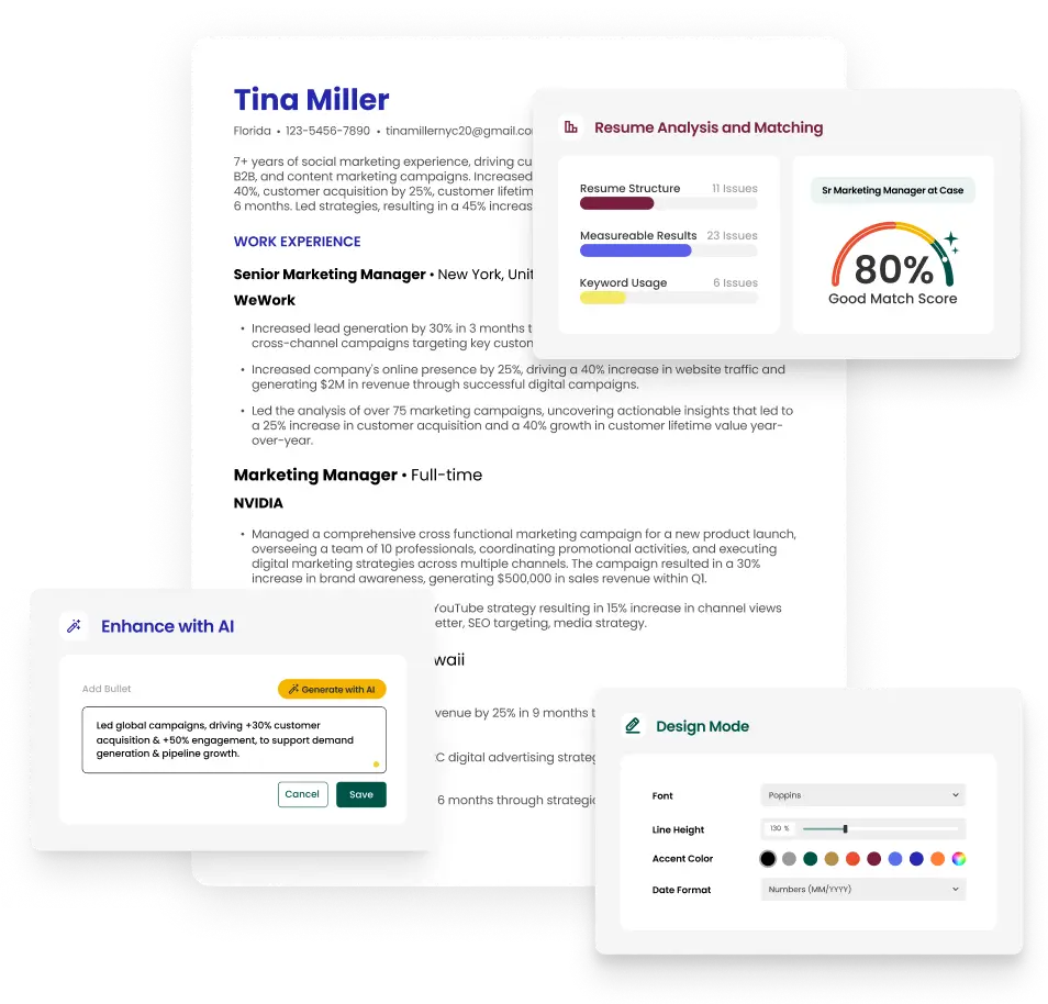
Build a Resume for Materials Engineer

The resume builder that gets results.

  • Get clear feedback so you look as qualified as you are
  • Align your resume with the job to get further in the process, faster
  • Take the guesswork out of resume writing

Explore Related Job Searches

© 2026 Teal Labs, Inc
Privacy PolicyTerms of Service