Materials Engineer Jobs

1,587 jobs found — updated daily

Process Engineer

Applied Materials•Santa Clara, CA
•$147,000 - $202,500

About The Position

Applied Materials is hiring a Process Engineer to design and optimize manufacturing processes for display and semiconductor manufacturing technologies. The role involves collecting and analyzing data, characterizing hardware, troubleshooting engineering issues, measuring film properties, preparing technical documentation, and working with customers to resolve concerns. The engineer also collaborates with vendors and suppliers and helps implement new technologies and products, partnering with global R&D teams on research and development projects. The position focuses on advanced cleaning and drying methods, including development of cleaning procedures and specifications for new product introduction, particularly for parts used in post-clean thin-film deposition applications. The engineer leads technical work and interfaces with internal teams, customers, and vendors; coordinates projects and personnel; trains and develops engineers and technicians; and directs safety, quality, and engineering training. Responsibilities also include leading investigations and improvement programs, supporting statistical process control and design of experiments, and ensuring cleaning, manufacturing, and equipment operations follow required standards and procedures. The position is based in Santa Clara, California, is full-time and regular, and requires travel 20% of the time. Relocation is eligible. The stated salary range is $147,000 to $202,500. Candidates may also be eligible for bonus and stock awards, as applicable.

Requirements

  • Bachelor’s degree in Engineering or Science at minimum.
  • Ideally, 3–5 or more years of related experience in high-technology manufacturing, preferably in the semiconductor capital equipment or support industry.
  • Significant academic and industrial expertise focused on using and developing advanced cleaning and drying methods.
  • Familiarity with bespoke selective chemistries, including acids, alkalis, and detergents, for wet and dry part cleaning, selective etch, passivation, and surface modification.
  • Experience managing, processing, and inspecting chamber materials such as steels, aluminum alloys, titanium alloys, nickel alloys, quartz, ceramics, and polymers.
  • Deep understanding and experience in metrology of new-part cleaning performance, including microscopy, surface roughness, CMM critical dimensions, ICPMS/VPD, LPC and bench-top particle quantification, emissivity, TXRF, SEM-EDX, laser scatter, and XPS.
  • Understanding of bath control regimes, including titration, pH, temperature, resistivity, flow, and etch rate for determining solution replacement timing.
  • Knowledge of selecting and optimizing surface agitation technologies.
  • Skill in designing and producing cleaning fixtures and equipment for advanced cleaning of recessed or internal surfaces.
  • Ability to critically examine specifications, tolerances, and technical drawings.
  • Knowledge of cleanroom protocols and advanced microcontamination.
  • Familiarity with wastewater treatment procedures.
  • Advanced understanding of semiconductor processes such as PVD, CVD, etch, ALD, diffusion, ALE, and CMP.
  • Ability to direct personnel and ensure adherence to quality, safety, and Copy Exact procedures.

Nice To Haves

  • A master’s degree or Ph.D.
  • More than five years of industrial experience.
  • Knowledge of hot-work processes such as flame polishing and kiln drying.
  • Applied Materials and OEM platform and part knowledge.

Responsibilities

  • Design and optimize manufacturing processes for display and semiconductor manufacturing technologies.
  • Collect and analyze data, perform hardware characterization, troubleshoot engineering issues, and measure film properties.
  • Generate technical documentation and engage with customers to resolve concerns.
  • Collaborate with vendors and suppliers and support the implementation of new technologies and products.
  • Establish new cleaning procedures and specifications for new product introduction, particularly for post-clean thin-film deposition applications.
  • Develop internal documents such as work order travelers, inventory records, and logs.
  • Establish priorities, manage and schedule cleaning projects, and deliver complex solutions on time.
  • Ensure engineering personnel complete required tasks on time and balance workloads across regions when needed.
  • Lead technical interfaces with internal teams, global external customers, and key vendors.
  • Train engineers and technicians to proficiency on assigned tasks; coach staff and develop succession plans.
  • Familiarize teams with wastewater treatment procedures and ensure technicians' assigned tasks are completed on time.
  • Direct safety, policy, and engineering training.
  • Lead CAPA, FOI, and FMEA investigations related to cleaning issues and present findings to customers.
  • Develop and lead advanced statistical analysis, statistical process control, and design of experiments.
  • Direct product improvement and cost reduction programs.
  • Ensure Copy Exact procedures and practices are maintained and implemented.
  • Ensure equipment and manufacturing operations meet required quality and safety standards.
  • Appraise employee performance in accordance with company policies.

Benefits

  • Comprehensive benefits package
  • Potential eligibility for a bonus program
  • Potential eligibility for a stock award program
  • Relocation eligibility

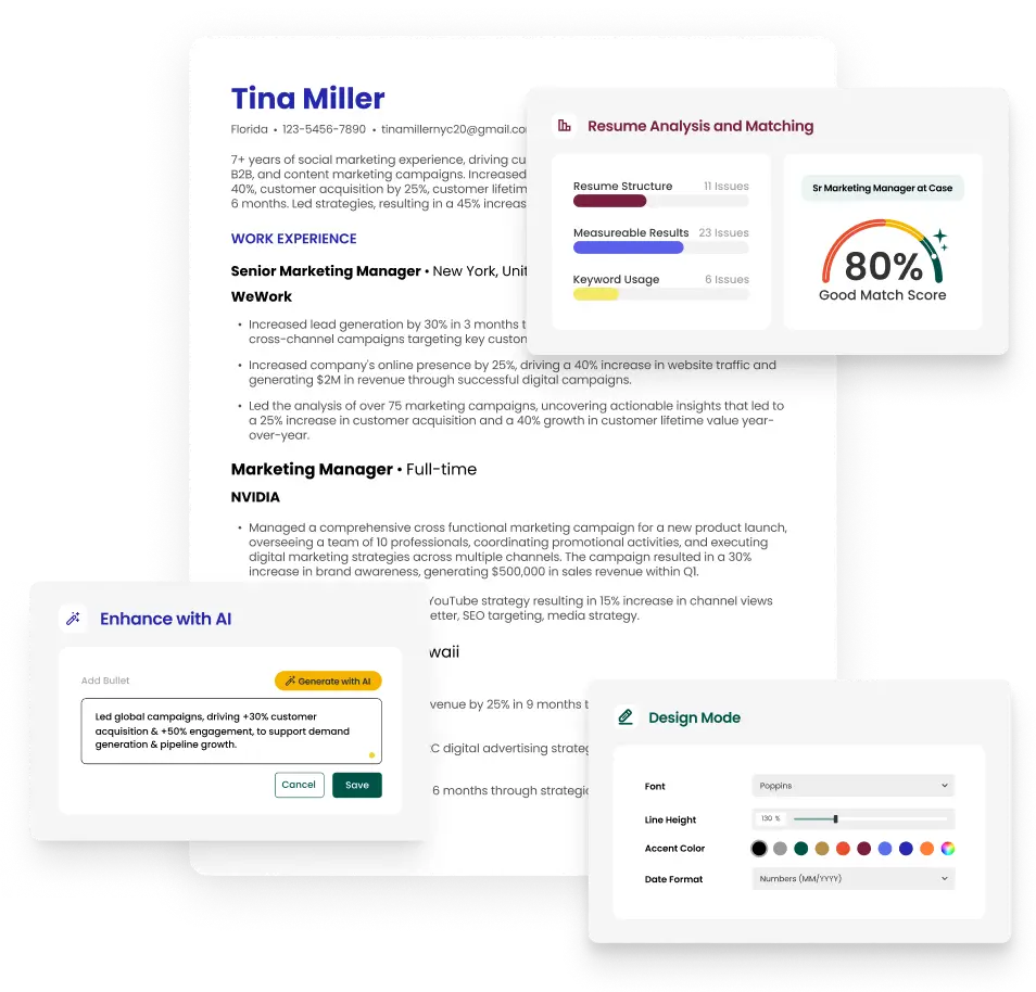
Build a Resume for Materials Engineer

The resume builder that gets results.

  • Get clear feedback so you look as qualified as you are
  • Align your resume with the job to get further in the process, faster
  • Take the guesswork out of resume writing

Explore Related Job Searches

© 2026 Teal Labs, Inc
Privacy PolicyTerms of Service